Transistors
Introduction
Transistors make our electronics world go ‘round. They’re critical as a control source in just about every modern circuit. Sometimes you see them, but more-often-than-not they’re hidden deep within the die of an integrated circuit. In this tutorial we’ll introduce you to the basics of the most common transistor around: the bi-polar junction transistor (BJT).

In small, discrete quantities, transistors can be used to create simple electronic switches, digital logic, and signal amplifying circuits. In quantities of thousands, millions, and even billions, transistors are interconnected and embedded into tiny chips to create computer memories, microprocessors, and other complex ICs.
Covered In This Tutorial
After reading through this tutorial, we want you to have a broad understanding of how transistors work. We won’t dig too deeply into semiconductor physics or equivalent models, but we’ll get deep enough into the subject that you’ll understand how a transistor can be used as either a switch or amplifier.
This tutorial is split into a series of sections, covering:
- Symbols, Pins, and Construction – Explaining the differences between the transistor’s three pins.
- Extending the Water Analogy – Going back to the water analogy to explain how a transistor acts like a valve.
- Operation Modes – An overview of the four possible operating modes of a transistor.
- Switches – Application circuits showing how transistors are used as electronically controlled switches.
There are two types of basic transistor out there: bi-polar junction (BJT) and metal-oxide field-effect (MOSFET). In this tutorial we’ll focus on the BJT, because it’s slightly easier to understand. Digging even deeper into transistor types, there are actually two versions of the BJT: NPN and PNP. We’ll turn our focus even sharper by limiting our early discussion to the NPN. By narrowing our focus down – getting a solid understanding of the NPN – it’ll be easier to understand the PNP (or MOSFETS, even) by comparing how it differs from the NPN.
Symbols, Pins, and Construction
Transistors are fundamentally three-terminal devices. On a bi-polar junction transistor (BJT), those pins are labeled collector (C), base (B), and emitter (E). The circuit symbols for both the NPN and PNP BJT are below:
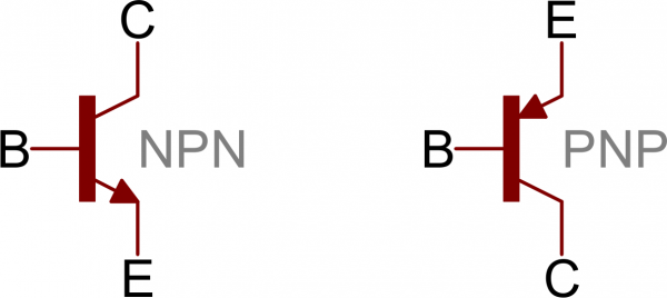
The only difference between an NPN and PNP is the direction of the arrow on the emitter. The arrow on an NPN points out, and on the PNP it points in. A useful mnemonic for remembering which is which is:
NPN: Not Pointing iN
Backwards logic, but it works!
Transistor Construction
Transistors rely on semiconductors to work their magic. A semiconductor is a material that’s not quite a pure conductor (like copper wire) but also not an insulator (like air). The conductivity of a semiconductor – how easily it allows electrons to flow – depends on variables like temperature or the presence of more or less electrons. Let’s look briefly under the hood of a transistor. Don’t worry, we won’t dig too deeply into quantum physics.
Transistor Structure and Operation
Transistors are built by stacking three different layers of semiconductor material together. Some of those layers have extra electrons added to them (a process called “doping”), and others have electrons removed (doped with “holes” – the absence of electrons). A semiconductor material with extra electrons is called an n-type (n for negative because electrons have a negative charge) and a material with electrons removed is called a p-type (for positive). Transistors are created by either stacking an n on top of a p on top of an n, or p over n over p.

Simplified diagram of the structure of an NPN. Notice the origin of any acronyms?
With some hand waving, we can say electrons can easily flow from n regions to p regions, as long as they have a little force (voltage) to push them. But flowing from a p region to an n region is really hard (requires a lot of voltage). But the special thing about a transistor is the fact that electrons can easily flow from the p-type base to the n-type collector as long as the base-emitter junction is forward biased (meaning the base is at a higher voltage than the emitter).

The NPN transistor is designed to pass electrons from the emitter to the collector (so conventional current flows from collector to emitter). The emitter “emits” electrons into the base, which controls the number of electrons the emitter emits. Most of the electrons emitted are “collected” by the collector, which sends them along to the next part of the circuit.
A PNP works in a same but opposite fashion. The base still controls current flow, but that current flows in the opposite direction – from emitter to collector. Instead of electrons, the emitter emits “holes” (a conceptual absence of electrons) which are collected by the collector.
The transistor is kind of like an electron valve. The base pin is like a handle you might adjust to allow more or less electrons to flow from emitter to collector. Let’s investigate this analogy further…
Extending the Water Analogy
If you’ve been reading a lot of electricity concept tutorials lately, you’re probably used to water analogies. We say that current is analogous to the flow rate of water, voltage is the pressure pushing that water through a pipe, and resistance is the width of the pipe.
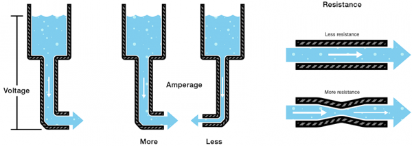
Unsurprisingly, the water analogy can be extended to transistors as well: a transistor is like a water valve – a mechanism we can use to control the flow rate.
There are three states we can use a valve in, each of which has a different effect on the flow rate in a system.
1) On – Short Circuit
A valve can be completely opened, allowing water to flow freely – passing through as if the valve wasn’t even present.

Likewise, under the right circumstances, a transistor can look like a short circuit between the collector and emitter pins. Current is free to flow through the collector, and out the emitter.
2) Off – Open Circuit
When it’s closed, a valve can completely stop the flow of water.

In the same way, a transistor can be used to create an open circuit between the collector and emitter pins.
3) Linear Flow Control
With some precise tuning, a valve can be adjusted to finely control the flow rate to some point between fully open and closed.

A transistor can do the same thing – linearly controlling the current through a circuit at some point between fully off (an open circuit) and fully on (a short circuit).
From our water analogy, the width of a pipe is similar to the resistance in a circuit. If a valve can finely adjust the width of a pipe, then a transistor can finely adjust the resistance between collector and emitter. So, in a way, a transistor is like a variable, adjustable resistor.
Amplifying Power
There’s another analogy we can wrench into this. Imagine if, with the slight turn of a valve, you could control the flow rate of the Hoover Dam’s flow gates. The measly amount of force you might put into twisting that knob has the potential to create a force thousands of times stronger. We’re stretching the analogy to its limits, but this idea carries over to transistors too. Transistors are special because they can amplify electrical signals, turning a low-power signal into a similar signal of much higher power.
Kind of. There’s a lot more to it, but that’s a good place to start! Check out the next section for a more detailed explanation of the operation of a transistor.
Operation Modes
Unlike resistors, which enforce a linear relationship between voltage and current, transistors are non-linear devices. They have four distinct modes of operation, which describe the current flowing through them. (When we talk about current flow through a transistor, we usually mean current flowing from collector to emitter of an NPN.)
The four transistor operation modes are:
- Saturation – The transistor acts like a short circuit. Current freely flows from collector to emitter.
- Cut-off – The transistor acts like an open circuit. No current flows from collector to emitter.
- Active – The current from collector to emitter is proportional to the current flowing into the base.
- Reverse-Active – Like active mode, the current is proportional to the base current, but it flows in reverse. Current flows from emitter to collector (not, exactly, the purpose transistors were designed for).
To determine which mode a transistor is in, we need to look at the voltages on each of the three pins, and how they relate to each other. The voltages from base to emitter (VBE), and the from base to collector (VBC) set the transistor’s mode.
Let’s look at all four transistor modes individually; we’ll investigate how to put the device into that mode, and what effect it has on current flow.
Note: The majority of this page focuses on NPN transistors. To understand how a PNP transistor works, simply flip the polarity or > and < signs.
Saturation Mode
Saturation is the on mode of a transistor. A transistor in saturation mode acts like a short circuit between collector and emitter.

To achieve saturation mode, VBE must be greater than a threshold voltage. There are many abbreviations for this voltage drop – Vth, Vγ, and Vd are a few. We'll use VBE(sat). The actual value varies among transistors (and even further by temperature). For a lot of transistors (at room temperature) we can estimate this drop to be about 0.6V–0.95V (depending on the base current applied).
The full story on saturation versus active mode is more complicated than just surpassing this threshold voltage, but it will suffice for now.
Another reality bummer: there won’t be perfect conduction between emitter and collector. A small voltage drop will form between those nodes. Transistor datasheets will define this voltage as CE saturation voltage VCE(sat) – a voltage from collector to emitter required for saturation. This value is usually around 0.05-0.2V. This value means that VC must be (at least) slightly greater than VE to get the transistor in saturation mode with current flowing from collector to emitter (C to E).
Another way to think about the action of a transistor in saturation, is that it's trying to bring the collector voltage as close as it can to the emitter voltage, just like a real short circuit would.
We will have more to say and reiterate about voltage drops, VCE and even VBE later.
Cutoff Mode
Cutoff mode is the opposite of saturation. A transistor in cutoff mode is off – there is no collector current, and therefore no emitter current. It almost looks like an open circuit.
To get a transistor into cutoff mode, the base voltage must be less than both the emitter and collector voltages. VBC and VBE must both be non-positive.
In reality, VBE can be anywhere between 0V and VBE(sat) (≈0.7V) to achieve cutoff mode.
Active Mode
We won't use active mode for this class, but you might want to know that it exists, since it's how amplifiers like your stereo work.
To operate in active mode, a transistor’s VBE must be greater than zero and VBC must be negative. Thus, the base voltage will be be less than the collector, but greater than the emitter. That also means the collector must be greater than the emitter (which we generally expect at this point).
Remember that we need a non-zero forward voltage from base to emitter (VBE) to even “turn on” the transistor (much like an LED). But so long as VBE is not so high that the transistor is saturated (meaning: we are keeping VB in check), then we can drive some interesting behaviors.
Note: We won't use this part on the Active Mode for class, and it's not critical for you to learn or remember it. However, I recommend reading it at least once so that you have made a complete pass over the transistor's behaviors.
Amplifying in Active Mode
Active mode is the most powerful mode of the transistor because it turns the device into an amplifier. Current going into the base pin amplifies current going into the collector and out the emitter.
Our shorthand notation for the gain (amplification factor) of a transistor is β (you may also see it as βF, or hFE). β linearly relates the collector current (IC) to the base current (IB):

The actual value of β varies by transistor. It’s usually around 100, but can range from 50 to 200…even 2000, depending on which transistor you’re using and how much current is running through it. If your transistor had a β of 100, for example, that’d mean an input current of 1mA into the base could produce 100mA current through the collector.

Active mode model. VBE = Vth, and IC = βIB.
What about the emitter current, IE? In active mode, the collector and base currents go into the device, and the IE comes out. Because of conservation of charge (more on this later), the emitter current (output) must be the sum of the base and collector currents (inputs): IE = IC+IB.
To reiterate, the point here is that relatively small changes (in current) at the base (i.e., those caused by your voice moving a small wire near a magnet on your phone) are amplified by a much larger (linearly proportional) current at the collector. Cool!
Achieving Saturation
As a brief aside, do you want to know how we achieve saturation when it seems like active mode should rule the day? Read on!
Suppose the linear relation IC = βIB held always and forever. That would imply that we could make the current into the collector as large as we want so long as we could increase the base current enough.
Because Ohm's Law tells us the voltage drop across the resistor linearly depends on the current through it, that would also mean we could make the voltage drop across the resistor as big as we want. Kirchhoff's Voltage Law tells us that's not true: we can only drop from the "high" side of the resistor down to the "low" side (i.e., +5V down to ground). Because there is an upper limit on the voltage drop, there must be an upper limit on the current through the collector to the emitter. Once IB has gotten high enough to reach that maximum IC, the transistor has entered saturation. Voila!
Reverse Active
Just as saturation is the opposite of cutoff, reverse active mode is the opposite of active mode. A transistor in reverse active mode conducts, even amplifies, but current flows in the opposite direction, from emitter to collector. The downside to reverse active mode is the β (βR in this case) is much smaller.
To put a transistor in reverse active mode, the emitter voltage must be greater than the base, which must be greater than the collector (VBE<0 and VBC>0).
Reverse active mode isn’t usually a state in which you want to drive a transistor. It’s good to know it’s there, but it’s rarely designed into an application.
Relating to the PNP
After everything we’ve talked about on this page, we’ve still only covered half of the BJT spectrum. What about PNP transistors? PNP’s work a lot like the NPN’s – they have the same four modes – but everything is turned around. To find out which mode a PNP transistor is in, reverse all relative voltage values.
To put it more simply, with insufficient voltage at the base of an NPN transistor, it is in cutoff mode (like an open switch). However, with insufficient voltage at the base of a PNP transitor, it's in saturation mode (like a closed switch). Conversely, with sufficient voltage at the base of an NPN transistor, it enters saturation mode (like a closed switch), but when a sufficient voltage is applied to the base of the PNP transistor, it enters cutoff mode (like the open switch). Go figure.
Another opposing characteristic of the NPNs and PNPs is the direction of current flow. In active and saturation modes, current in a PNP flows from emitter to collector. This means the emitter must generally be at a higher voltage than the collector.
If you’re burnt out on conceptual stuff, take a trip to the next section. The best way to learn how a transistor works is to examine it in real-life circuits. Let’s look at some applications!
Switches
One of the most fundamental applications of a transistor is using it to control the flow of power to another part of the circuit – using it as an electric switch. Driving it in either cutoff or saturation mode, the transistor can create the binary on/off effect of a switch.
Transistor switches are critical circuit-building blocks; they’re used to make logic gates, which go on to create microcontrollers, microprocessors, and other integrated circuits. Below are a few example circuits.
Transistor Switch
Let’s look at the most fundamental transistor-switch circuit: an NPN switch. Here we use an NPN to control a high-power LED:
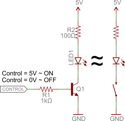
Our control input flows into the base, the output is tied to the collector, and the emitter is kept at a fixed voltage.
While a normal switch would require an actuator to be physically flipped, this switch is controlled by the voltage at the base pin. A microcontroller I/O pin, like those on an Arduino, can be programmed to go high or low to turn the LED on or off.
When the voltage at the base is greater than 0.6V (or whatever your transistor’s Vth might be), the transistor starts saturating and looks like a short circuit between collector and emitter. When the voltage at the base is less than 0.6V the transistor is in cutoff mode – no current flows because it looks like an open circuit between C and E.
The circuit above is called a low-side switch, because the switch – our transistor – is on the low (ground) side of the circuit. Alternatively, we can use a PNP transistor to create a high-side switch:
>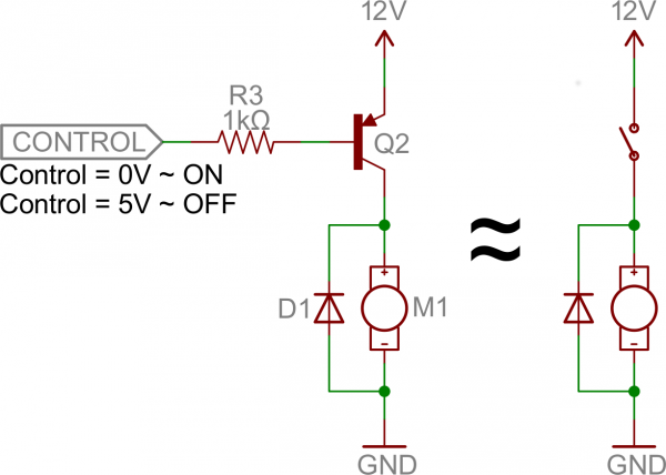
Similar to the NPN circuit, the base is our input, and the emitter is tied to a constant voltage. This time however, the emitter is tied high, and the load is connected to the transistor on the ground side.
This circuit works just as well as the NPN-based switch, but there’s one huge difference: to turn the load “on” the base must be low. This can cause complications, especially if the load’s high voltage (VCC in this picture) is higher than our control input’s high voltage. For example, this circuit wouldn’t work if you were trying to use a 5V-operating Arduino to switch on a 12V motor. In that case it’d be impossible to turn the switch off because VB would always be less than VE.
Base Resistors!
You’ll notice that each of those circuits uses a series resistor between the control input and the base of the transistor. Don’t forget to add this resistor! A transistor without a resistor on the base is like an LED with no current-limiting resistor.
In a way, a transistor is sort of like a pair of interconnected diodes. We
need to "activate" (or technically,
The series resistor between our control source and the base limits current into the base. The base-emitter node can get its happy voltage drop of 0.6V, and the resistor can drop the remaining voltage. The value of the resistor, and voltage across it, will thus set the current.
The resistor needs to be large enough to effectively limit the current, but small enough to feed the base enough current. 1mA to 10mA will usually be enough, but check your transistor’s datasheet to make sure.
Digital Logic
Transistors can be combined to create all our fundamental logic gates: AND, OR, and NOT.
These gates (which we'll talk more about in the next class) form the basis
of operations on Boolean values, which you'll be familiar with from both C
(where they're written as &&, ||, and
!) as well as Scheme (where the operators are the more intellegible
and, or, and not).
In circuits for digital logic, a (continuous) voltage is used to represent
the (discrete) Boolean values you are more accustomed to seeing in
programs. One possible convention might be that +0V (or Ground/GND) represents "off" or
false, while +5V represents "on" or true. In the
following, we look at how to use transistors in circuits to code these values
and combine them with the typical Boolean operators, AND, OR, and NOT.
(Note: These days MOSFETS are more likely to be used to create logic gates than BJTs. MOSFETs are more power-efficient, which can make them a better choice.)
Inverter
Here’s a transistor circuit that implements an inverter, or NOT gate:
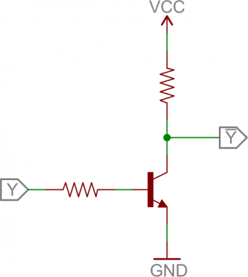
An inverter built out of transistors.
Here a high voltage into the base will turn the transistor on, which will effectively connect the collector to the emitter. Since the emitter is connected directly to ground, the collector will be as well (though it will be slightly higher, somewhere around VCE(sat) ~ 0.05-0.2V). If the input is low, on the other hand, the transistor looks like an open circuit, and the output is pulled up to VCC.
(This is actually a fundamental transistor configuration called common emitter. In this circuit the emitter is tied to a voltage common to both the base and emitter (usually ground). The base becomes the signal input, and the collector becomes the output.)
AND Gate
Here are a pair of transistors used to create a 2-input AND gate:
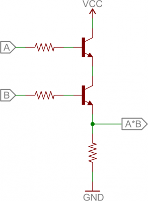
2-input AND gate built out of transistors.
If either transistor is turned off, then the output at the second transistor’s emitter will be pulled low (they are disconnected from VCC). If both transistors are “on” (bases both high), then the output of the circuit is also high.
OR Gate
And, finally, here’s a 2-input OR gate:
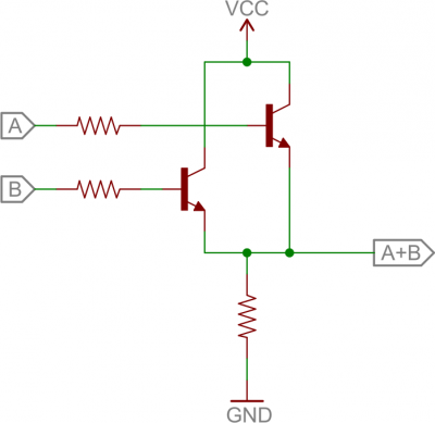
2-input OR gate built out of transistors.
In this circuit, if either (or both) A or B are high, that respective transistor will turn on, and pull the output high. If both transistors are off, then the output is pulled low through the resistor.
Kirchhoff's Law
In order to use transistors to control other components, it's important to understand how Kirchhoff's Voltage law apply to circuits involving transistors.
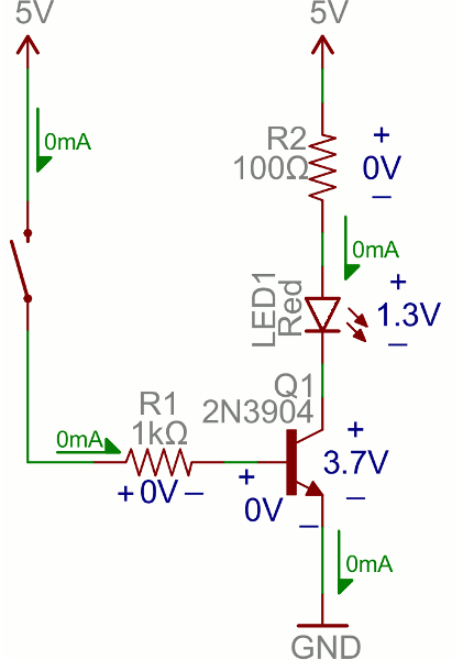
Let us take a closer look at the transistor circuit shown before in the state when the switch is closed in order to make sure we understand the currents and voltage drops.

The analysis begins with the 2N3904 transistor and its datasheet.
We would find that VBE(sat) is 0.7V, so we indeed see that is the voltage drop across the base and emitter terminals. By Kirchhoff's Voltage Law, because the base is tied "high" (when the switch is closed) to +5V, that leaves a voltage drop across the resistor as 5V–0.7V = 4.3V. We can then use Ohm's Law either to figure out the necessary resistance (in order to respect the current limit) or calculate the current (when given a resistance value). Taking the resistance of R1 as given at 1KΩ, we find that I = 4.3V/1kΩ = 4.3mA.
Considering the other path, the datasheet would tell us that VCE(sat) is 0.15V, which explains the voltage drop across the collector and emitter terminals. With a red LED having a 1.85V voltage drop, that leaves 5V–0.15V–1.85V = 3.0V across the resistor (R2). If we need to limit the current through the resistor and/or transistor, we would use this voltage to determine the necessary resistance by Ohm's Law. Taking the resistance of R2 as given, we find the current from the +5V supply to the collector is I = 3.0V/100Ω = 30mA.
Kirchhoff's Current Law
You might then notice that the current from the emitter to ground rail is the sum of the two "input" currents on the transistor: I = 4.3mA+30mA = 34.3mA. It turns out this is related to Kirchhoff's other law:
the sum of currents into a junction equals the sum of the currents out of the junction
This is known as Kirchhoff's Current Law (KCL). You saw the application of this earlier when we wrote IE = IC+IB.
We won't use that as much for this class, since it is the voltage levels that correspond to the binary (ON or OFF) states of interest for digital logic and computer design.
Conclusion
With the end of this reading, you should understand:
- the difference between NPN and PNP transistors
- the basics of how to use a transistor as a switch (i.e., saturation and cut-off modes),
- how to wire transistors into logic gates (i.e., AND, OR, NOT), and
- how to measure current through basic circuits and account for the voltage drop of resistors, LEDs, and transistors using Ohm's Law and Kirchhoff's Laws.